| Pin | Symbol | Function |
|---|---|---|
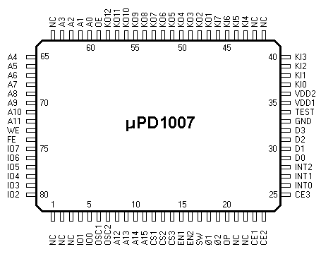
| 75..80, 4,5 | IO7..IO0 | bi-directional data bus |
| 6,7 | OSC1,OSC2 | ceramic resonator 910kHz, OSC2 is the output from the inverting oscillator amplifier |
| 8..11 | A12..A15 | address bus |
| 12..14 | CS1..CS3 | Chip select signals for three additional memory banks, active low. CS1: FA-80 interface CS2,CS3: single bit output port CNTL in the gate array uPD65005G-045 |
| 15 | EN1 | Single bit output port, low level turns the system power on. |
| 16 | EN2 | Single bit output port, drives the INT0 interrupt input allowing software triggered interrupts. |
| 17 | SW | Power switch input, connected either to VDD1 (power on) or to GND (power off). |
| 18,19 20 23..25 29..32 | Ø1,Ø2 OP CE1..CE3 D0..D3 | LCD controller bus, similar as in the Casio FX-700P, all signals use negative logic, pins CE2 and CE3 are not connected in the FX-8000G |
| 26 | INT0 | interrupt input, driven from the pin EN2 |
| 27 | INT1 | interrupt input, receives low level pulses from the pin 27 of the HD44352 LCD controller chip |
| 28 | INT2 | interrupt input, used by the FA-80 interface |
| 33 | GND | positive supply voltage |
| 34 | TEST | |
| 35 | VDD1 | permanent negative supply voltage |
| 36 | VDD2 | switched negative supply voltage |
| 37..40, 43..46 | KI0..KI7 | keyboard matrix input port, can be accessed through the KI register |
| 47..58 | KO1..KO12 | keyboard matrix output port, controlled by the KO register |
| 59 | OE | bus read signal, active low |
| 60..63, 65..72 | A0..A11 | address bus |
| 73 | WE | bus write signal, active low |
| 74 | FE | memory chip select signal, active low |
Quelle: Casio fx-8000G - hardware